Research
1. Design and fabrication of photonic nanostructures
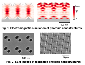 To realize nanophotonic devices with completely new functionalities, it is necessary to establish design methods of nanostructures with desired functionalities and fabrication techniques to reproduce the designed nanostructures. In our laboratory, we propose and design novel photonic nanostructures by using multiple electromagnetic simulation methods or by establishing an original theoretical analysis method (Fig. 1). In addition, we realize the fabrication of the designed structures with sub-nanometer-level accuracy by using state-of-the-art nano-processing equipment such as electron-beam lithography and plasma etching systems (Fig. 2).
2. High-power high-functionality photonic-crystal surface-emitting lasers
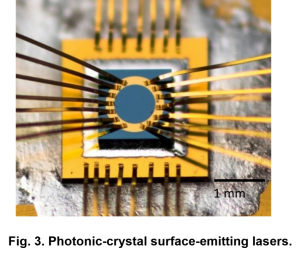
By using a large-area optical resonance supported by photonic nanostructures as a resonator for lasing oscillation, high-power narrow-divergence single-mode semiconductor lasers (photonic-crystal surface-emitting lasers: PCSELs) can be realized. In our laboratory, we aim to realize unprecedented functionalities in PCSELs, such as kW-class operation, short-pulse generation, 2D beam-scanning, and high-speed modulation, for a wide variety of applications such as Light detection and ranging (LiDAR), laser micro-processing, and intersatellite optical communications (Fig. 3).
3. Non-Hermitian photonic devices based on photonic nanostructures
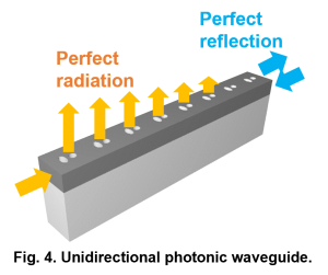 In photonic nanostructures, light propagating inside them loses a part of its energy when radiated in the vertical direction. In other words, photonic nanostructures are “non-Hermitian” systems, where the conservation law of energy does not hold, and are expected to exhibit counter-intuitive physical phenomena that differ from Hermitian systems. For example, by appropriately designing photonic nanostructures, it is possible to realize unique optical waveguides that perfectly radiate light in the vertical direction when light is incident from one direction, while perfectly reflect light when incident from the opposite direction (Fig. 4). By taking advantage of such non-Hermitian nature, we aim to propose and demonstrate novel nanophotonic devices that transcend the limits of conventional photonics.